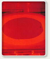
Silicon epitaxy (epi) is deposited onto silicon wafers used to manufacture semiconductors devices, such as MOSFETS or integrated circuits (ICs). We supply up to 150mm but capable of 200mm, please enquire. A typical customer may not have internal epitaxy capability, or has the internal capability but has exceeded his capacity
Polysilicon coating services for silicon carbide and quartz products for use in single wafer and cluster tool RTP, CVD, and Etch chambers. |
Outsourcing of think film deposition semiconductor processing can be an important business strategy for a semiconductor manufacturer. This is true regardless of the volatile semiconductor industry cycle. During cyclical downturns in demand, outsourcing can allow a semiconductor manufacturer to reduce operating costs by temporarily idling in-house capacity while maintaining both throughput and quality. During boom periods, outsourcing can provide extra capacity on a regular or periodic basis. A third benefit of outsourcing is to provide backup production capability in the event of a sudden and unexpected loss of internal capability. |
Reaction Technology Inc. services include single layers, growth on buried layers and patterns as well as advanced device structures on wafers up to 200mm in diameter.
Our range of silicon epitaxial services is unparalleled. Committed to meeting our customers epitaxial needs from production development to large volume production, we offer more than a service, we offer a long-term relationship.
We've combined equipment and process expertise to provide epi wafers with precise and uniform thickness and resistivity, reduced stress, excellent morphology and low particulate counts. Our success is ultimately measured by the high satisfaction of our customers.
We provide basic epi technologies and also have expertise and experience in demanding technologies such as CMOS, CCD, BiCMOS, MOSFETS, IGBT's, and force sensors. We provide quick turn-around on 100mm to 200mm wafers for volumes ranging from R&D to full scale production. Our service includes:
Volume
Production
24 hour turn-around under optimized conditions with in-depth characterization to meet demanding foundry Schedules
Buried Layer
Epitaxial Processing
Growth of epitaxial layers over the customer's buried layers without disrupting stepper recognition
Short Run
Epitaxial Processing
Pilot and Engineering Lots
Specialized
Epitaxial Processing
Epitaxial layers on SIMOX and SOS substrates.
Developmental
Services
Processes and device structures developed using rigorous experimental matrices |


